
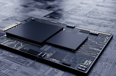
In the post-Moore era, the performance improvement of semiconductor chips no longer relies solely on the shrinking of wafer process nodes. Advanced chip packaging technology has become a core track to break through the physical limits of single-chip performance, increase integration density, reduce power consumption, and control manufacturing costs. From traditional 2D packaging to 2.5D intermediate layer packaging, and then to the emerging 3D stacked packaging and panel-level packaging in 2025–2026, the global chip packaging industry is undergoing a comprehensive technological revolution.
Benefiting from the booming demand for AI large model computing, high-bandwidth memory (HBM), and 5G/6G high-speed communication chips, new packaging technologies with high density, high bandwidth, low latency, and low cost are rapidly iterating. This article sorts out the most representative latest chip packaging technologies, analyzes their technical advantages, industrial landing status, and application boundaries, and summarizes the future evolution direction of the advanced packaging industry.
1. Industry Background: Advanced Packaging Becomes the Core Competition Track of Semiconductors
In recent years, the slowdown of wafer process iteration and the skyrocketing cost of advanced lithography processes have forced the semiconductor industry to shift its technological breakthrough focus from front-end manufacturing to back-end packaging and testing. Traditional packaging forms such as QFP and BGA can no longer meet the ultra-high integration and ultra-high bandwidth requirements of AI accelerators, high-end GPUs, and computing chips.
Advanced packaging technologies represented by 2.5D/3D stacking and panel-level packaging have realized heterogeneous integration of different process chips, HBM memory, and functional dies. They effectively solve the problems of insufficient inter-chip transmission bandwidth, large signal delay, and high power consumption, and have become the standard configuration for high-end chip mass production in 2025–2026.
2. Mainstream Latest Chip Packaging Technologies (2025–2026)
2.1 CoWoS Packaging: The Dominant Solution for High-End AI Chips
CoWoS (Chip on Wafer on Substrate) is currently the most mature and widely mass-produced 2.5D advanced packaging technology, and it is the core packaging solution for mainstream high-end AI GPUs and computing chips.
Different from traditional packaging, CoWoS adopts a silicon intermediate layer to realize interconnection between multiple dies and HBM. It features ultra-high wiring density, extremely low signal delay, and excellent heat dissipation performance. In 2026, TSMC’s upgraded CoWoS process achieves mass production of 5.5x reticle size products, with a mass production yield rate exceeding 98%, which can integrate more computing dies and HBM stacks in a single package to support larger-scale AI model computing.
Core Advantages: Ultra-high interconnection bandwidth, stable high-frequency signal transmission, mature mass production process, excellent thermal management performance. Main Applications: High-end AI GPU, large-scale computing chips, data center accelerator chips.
2.2 3D SoIC Packaging: Next-Generation 3D Stacking Technology
SoIC (System on Integrated Chips) is TSMC’s flagship 3D advanced packaging technology, which realizes atomic-level seamless stacking of multiple chips through ultra-fine pitch bonding, representing the highest level of current 3D heterogeneous integration.
Compared with traditional 2.5D packaging, SoIC completely abandons the limited interconnection mode of solder bumps. It achieves vertical stacking of dies through direct copper-to-copper bonding, with a bonding pitch reduced to the micron level. This technology greatly improves chip integration density, reduces inter-chip transmission distance and power consumption, and breaks the bandwidth bottleneck of 2.5D packaging.
Core Advantages: Ultra-high integration density, ultra-low latency, low power consumption, support for multi-layer heterogeneous stacking. Main Applications: High-end mobile SoC, ultra-high-performance computing chips, miniature sensor modules.
2.3 Hybrid Bonding: Core Bonding Technology for 3D Packaging Iteration
Hybrid Bonding is a key underlying technology for the iteration of advanced 3D packaging. It integrates copper conductive bonding and dielectric insulating bonding, realizing direct atomic-level fusion between wafer and wafer, die and die without solder bumps.
Traditional bump bonding has pitch limitations and parasitic impedance problems, while Hybrid Bonding can achieve ultra-fine pitch interconnection, effectively increasing the number of inter-channel connections per unit area. It greatly improves signal bandwidth and reduces contact resistance, and is the core technology supporting the large-scale popularization of 3D stacking packaging.
Core Advantages: Ultra-fine interconnection pitch, low contact impedance, high bandwidth, high stability. Main Applications: HBM high-bandwidth memory packaging, high-density 3D chip stacking, advanced sensor packaging.
2.4 FOPLP Panel-Level Packaging: Low-Cost High-Volume Packaging Solution
FOPLP (Fan-Out Panel Level Packaging) is a rapidly emerging panel-level advanced packaging technology in 2025–2026. It breaks the limitation of traditional circular wafer packaging and adopts a square large-size panel process for packaging and redistribution.
Compared with wafer-level packaging, FOPLP has an extremely high material utilization rate. The utilization rate of circular wafer packaging is only about 70%, while the square panel can reach more than 95%. The effective area of a single large panel is equivalent to 4–5 times that of a 12-inch wafer, which greatly improves production efficiency and reduces single-chip packaging costs.
Core Advantages: High material utilization, low manufacturing cost, high mass production efficiency, suitable for large-scale batch production. Main Applications: Consumer electronics chips, IoT modules, automotive electronic chips, mid-range communication chips.
2.5 CoPoS: New-Generation Panel-Level AI Packaging Technology
CoPoS (Chip on Panel on Substrate) is a new upgraded advanced packaging technology derived from CoWoS, which perfectly combines the high performance of 2.5D packaging and the low-cost advantage of panel-level packaging.
By changing the circular wafer carrier to a large-size square panel, CoPoS solves the problem of insufficient CoWoS production capacity and high cost. While maintaining high-precision multi-die integration and HBM matching capabilities, it achieves a substantial increase in production capacity, and is expected to become the mainstream cost-effective solution for mid-to-high-end AI chip packaging in 2027–2028.
Core Advantages: Ultra-high capacity output, balanced performance and cost, high area utilization. Main Applications: Mass-produced AI computing chips, edge computing modules, high-end consumer electronic chips.
3. Core Development Trends of Chip Packaging Technology (2025–2027)
3.1 From 2.5D to 3D Full-Scale Popularization
The industry is accelerating the transition from single 2.5D intermediate layer packaging to 3D three-dimensional stacked packaging. Technologies such as SoIC and Hybrid Bonding will gradually replace traditional bump interconnection processes, realizing higher-density heterogeneous integration and further breaking through chip performance bottlenecks.
3.2 Dual Track of High-End Performance and Low-Cost Mass Production
High-end markets such as AI computing will continue to iterate around CoWoS and 3D SoIC to pursue ultra-high bandwidth and ultra-low latency; consumer electronics and automotive electronics markets will rely on FOPLP and CoPoS panel-level packaging to achieve cost reduction and efficiency improvement, forming a differentiated competitive pattern.
3.3 Integration of Packaging and Testing Becomes Standard
With the continuous improvement of packaging integration, the difficulty of post-packaging testing increases synchronously. Highly matched pogo pin test fixtures and automated needle bed testing solutions have become essential supporting processes for advanced packaging mass production, realizing full-coverage testing of high-density pins, high-frequency signals, and multi-layer stacked chips.
3.4 Continuous Innovation of Packaging Materials and Equipment
New technologies such as glass interposer packaging and advanced packaging lithography are continuously iterating. The upgrading of equipment and materials further reduces the defect rate of advanced packaging and improves the stability of mass production.
4. Industry Challenges and Future Prospects
Although advanced chip packaging technologies are developing rapidly, the industry still faces multiple challenges: ultra-fine pitch bonding process difficulty, high equipment investment cost, heat dissipation bottleneck of high-density stacked chips, and high testing threshold for heterogeneous integrated modules.
In the next two years, with the continuous maturity of Hybrid Bonding and panel-level packaging processes, advanced packaging will further realize cost reduction and popularization. It will no longer be limited to high-end AI chips, but will be widely applied in automotive electronics, industrial control, high-speed communication, and smart sensing fields, becoming the core driving force for the sustainable development of the global semiconductor industry.
5. Conclusion
2025–2026 is a critical turning point for the chip packaging industry to move from traditional packaging to advanced heterogeneous integration. Multiple innovative technologies such as CoWoS, 3D SoIC, Hybrid Bonding, FOPLP, and CoPoS are reshaping the semiconductor industry pattern. The technological competition of future chips will no longer be limited to process node competition, and advanced packaging capability will become an important core competitiveness of semiconductor enterprises.
For manufacturing and testing engineers, mastering the technical characteristics and application scenarios of the latest advanced packaging is crucial to optimizing production processes, improving product yield, and reducing manufacturing costs.