Bay Area Semiconductor Expo | Haizhixiang Direct Factory
Shenzhen Haizhixiang Electronics at Bay Area Semiconduc […]


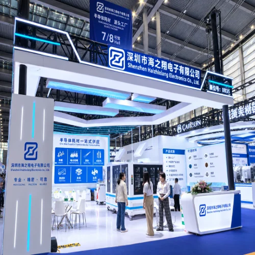
Shenzhen Haizhixiang Electronics at Bay Area Semiconduc […]
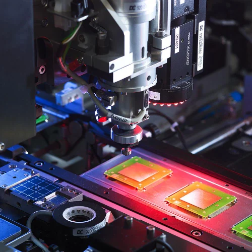
Semiconductor Rubber Suction Nozzles Made from Imported
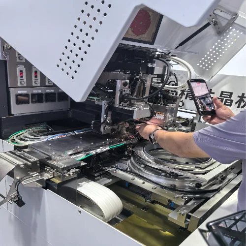
More Than a Supplier — Your Trusted Semiconductor Solut
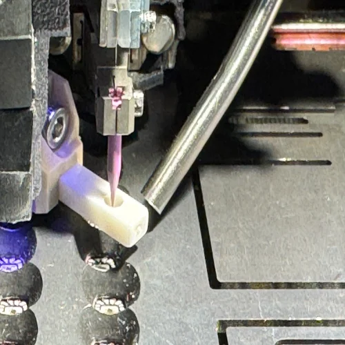
In semiconductor packaging and wire bonding processes,
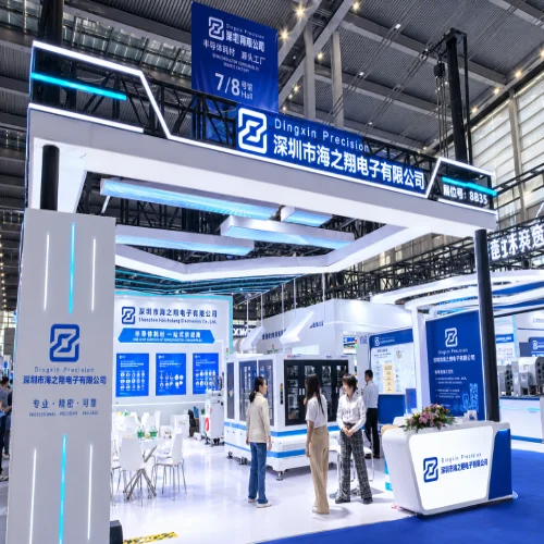
As the semiconductor, LED packaging, and electronics in
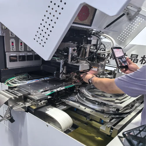
In semiconductor packaging and testing, high-quality co
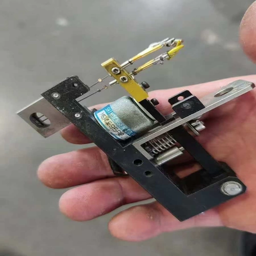
In semiconductor testing and electronics manufacturing,
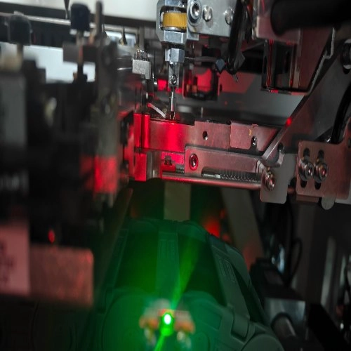
In precision manufacturing, nozzle performance can affe
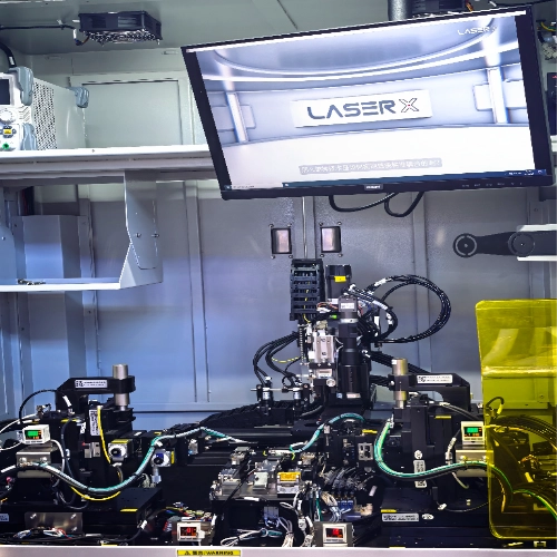
After the National Day holiday, production teams return
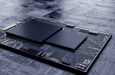
Driven by the explosive growth of AI computing power, high-speed communication, and miniaturized smart hardware, advanced chip packaging has become the core engine of semiconductor performance iteration and capacity expansion, gradually surpassing chip design and wafer manufacturing as the key bottleneck restricting high-end chip output. This article systematically analyzes the latest mainstream chip packaging technologies in 2025–2026, including CoWoS, 3D SoIC, Hybrid Bonding, FOPLP panel-level packaging, and CoPoS. It elaborates on technical principles, performance advantages, industrial application scenarios, and future development trends, providing professional references for semiconductor manufacturing, hardware R&D, and SMT testing engineers.